An X-ray diffractometer (XRD) is a powerful tool that provides cost-effective and non-destructive molecular structure studying of complex material matrices with minimal samples in many areas such as exploration, industrial production, pharmaceuticals, and archeology. The performance of both detectors and readout electronics determines the quality of the diffraction pattern. In applications requiring high detection accuracy, front-end readout electronics with a high signal-to-noise ratio (SNR) are extremely important.
The energy of injected X-rays is from 0.5 to 30 keV in these applications. A silicon strip detector is employed to realize this scientific objective. An ultra-low-noise front-end readout circuits are one of the key modules to read out weak current signals generated from silicon sensors. In most existing front-end readout electronic systems, charge-sensitive amplifiers (CSA) have proven to be good candidates for implementing low-noise analog front-ends. In this topology, a single-ended folded cascode amplifier is used as the core amplifier. To obtain high SNR, a high-order pulse shaper is required to filter the noise signals near the operational frequency and give more voltage gain. The optimal W/L ratio for the input transistors can be optimized according to the equivalent noise-charge formula. The schematic of the proposed ultra-low-noise analog front-ends is shown in Fig. 1.

Fig.1 The schematic of the proposed ultra-low-noise analog front-ends
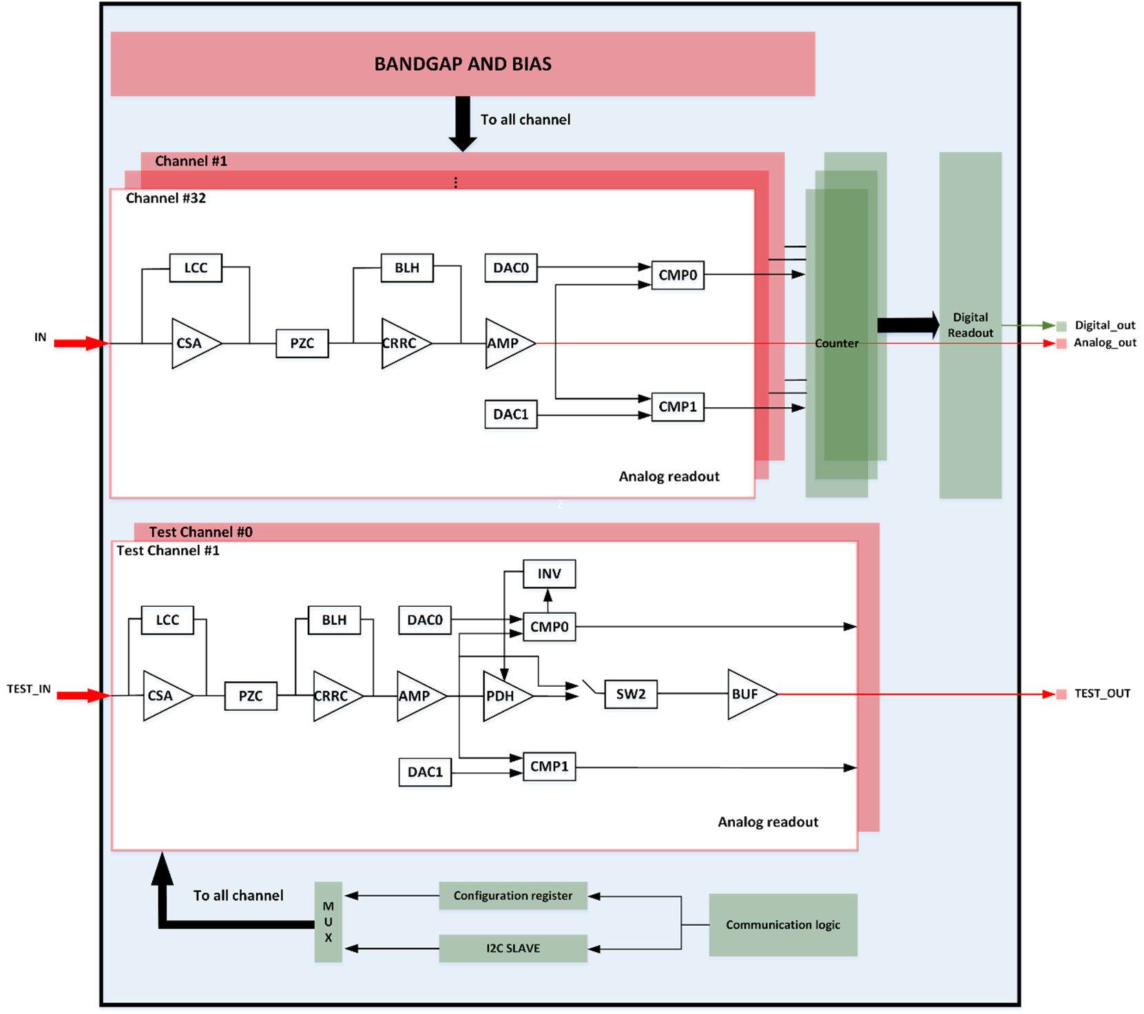
In our group, a project of developing a multichannel ultra-low-noise front-end readout application-specific integrated circuit (ASIC) for silicon microstrip detectors has been started since Jan. 2020. The trade-off design between low noise and high count rate is made in last two years. The diagram of the proposed ASIC is shown in Fig. 2.

Fig.2 The diagram of the proposed ASIC
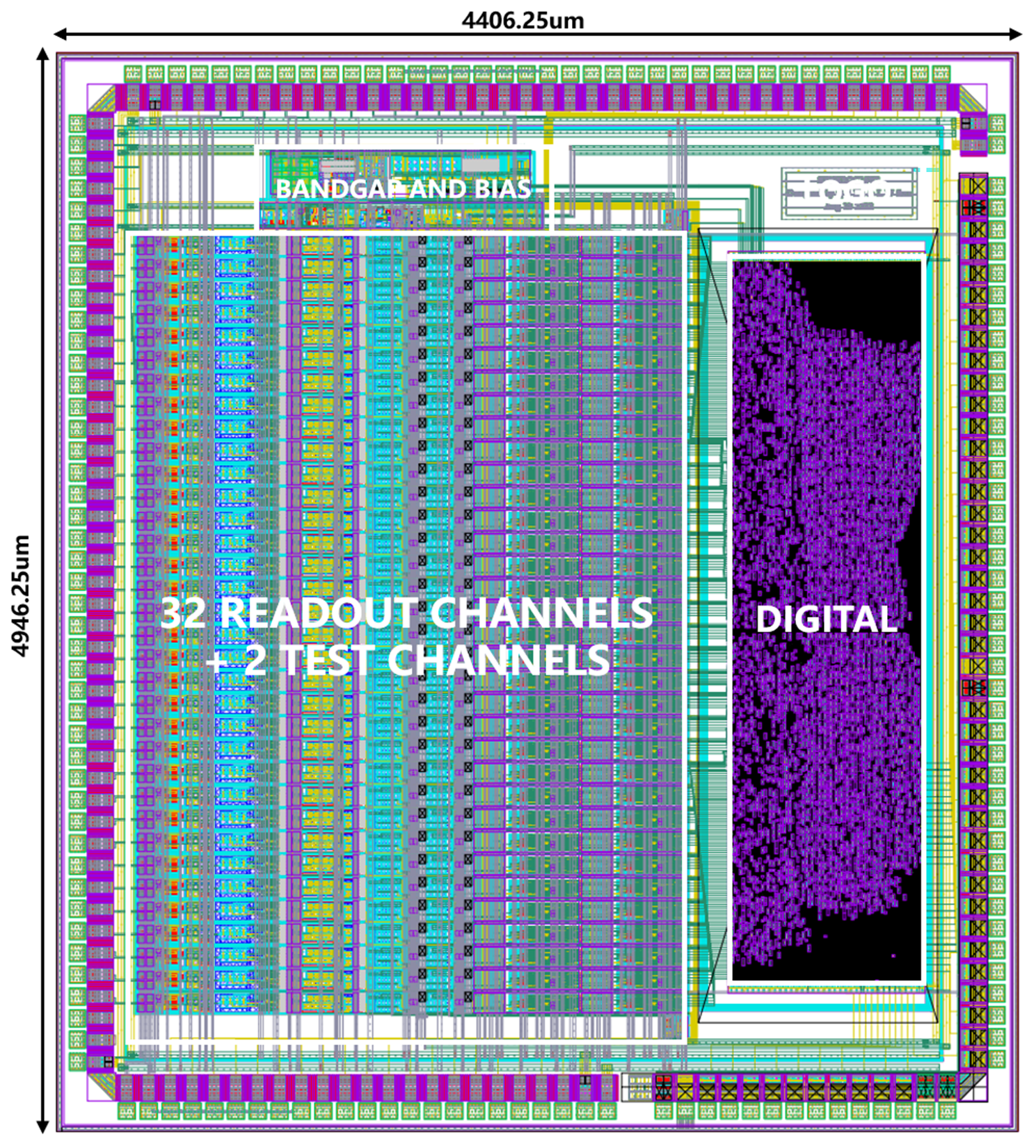
An ASIC prototype (named as SENSROC15V2) including 32 photon-count channels and 2 energy-resolving channels was designed in CMOS 0.35 μm mixed-signal 3.3 V process. The die size is 4.4 mm × 4.9 mm. Each channel mainly includes a charge-sensitive amplifier, a digital programmable pulse shaper, a baseline holder circuit, a leakage current compensation, and a discriminator. The chip is under fabrication.

Fig.2 The layout of the fabricated chip
The simulation results are obtained. The overview performance of the submitted ASIC is concluded in Table I.
Table I Overview performance of the taped-out ASIC
Parameter Name |
Experimental results |
Channel No. |
32 |
Dynamic Range(single channel) |
0.08 fC ~ 1.4fC |
ENC(single channel) |
32 e- + 5.2 e- / pF |
Power Dissipation: |
4.5 mW / channel |
For future work, electrical characterization of the ASIC will be measured. In addition, the ASIC will be connected to the multi-channel silicon strip for performance evaluation.
(Authors: Q . Xu, Reviewer: W. Gao)