【中文摘要】:在暗物质探测应用中,天基辐射探测系统需要一种高分辨高速多通路ADC。由于撞击粒子是随机的,采用事件驱动的前端读出电子学能够减小数据量,同时降低功耗。在这类应用中,对ADC的需求是:分辨率达到14位,采样率高于3MSps,单芯片通道数不少于16。2020年以来,我们实验室研究生提出了一种基于逐次逼近、单斜坡和TDC相结合的混合型ADC结构,很好地实现了这个技术需求。在一个单通路转换电路中,逐次逼近ADC为5位、单斜坡ADC为4位、TDC为5位,在100MHz时钟驱动下,能够在14位分辨率下达到3.4MSps的采样率,单路静态功耗为4mW。采用180纳米CMOS工艺完成了一款4通路原理样片的设计,目前已经投片制造。这种ADC结构,在牺牲采样率的情况下,可将分辨率提升至16位。同时,也能够轻松地扩展至128或256通路,集成在探测器前端读出ASIC中。这些特性使得这种ADC在高能物理实验和分子级生物医学成像等应用中有巨大潜力。
【English Text】:In the field of dark matter detection, particles arrive randomly. An event-driven ADC is required to construct energy-efficient front-end electronics for space-bone radiation detector systems. The requirements of the ADC are listed below: the resolution is 14 Bits; the sampling rate is larger than 3 Msps and the channel number is larger than 16. In our group, a novel hybrid ADC combining the techniques of SAR ADC, Single-slope ramp ADC and time-to-digital converter is proposed to perform the conversion of the voltage signals from a front-end readout ASIC to digital data. The ADC operates only when an event occurs, and remains in a standby state for the rest of the time so that the operation efficiency of the ADC is effectively improved and the power consumption is reduced.
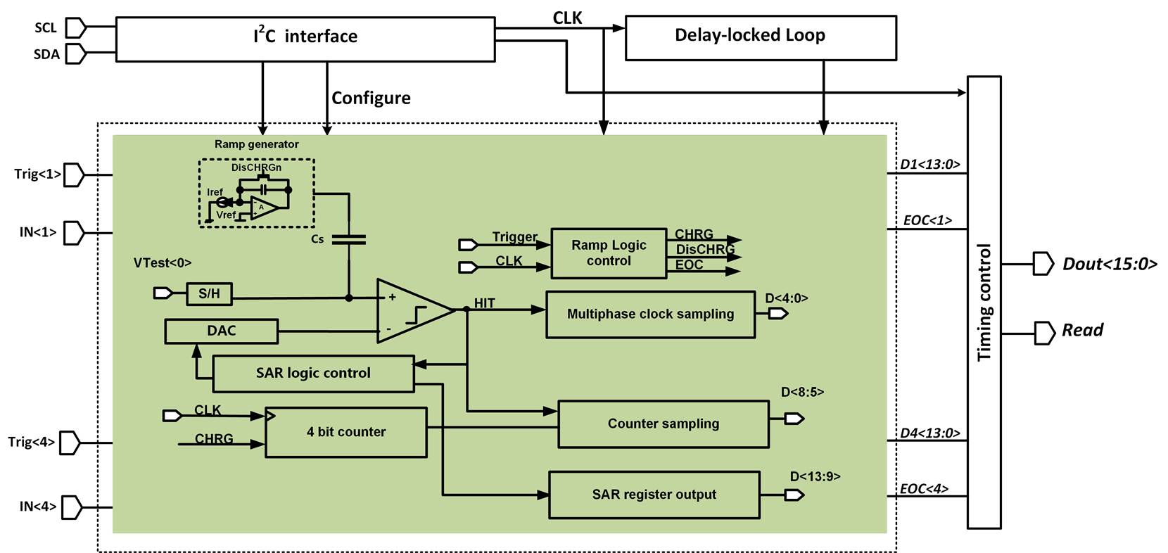
Fig.1 The diagram of an Event-Driven SAR/Ramp/TDC hybrid ADC.
The diagram of the proposed ADC is shown in Fig.1. A three-stage hybrid architecture which consists of 4-bit SAR ADC, 5-bit single-slope ramp ADC and 5-bit TDC are adopted to achieve a nominal 14-bit resolution. With a 100-MHz clock, the sampling rate is up to 3.4 Msps. An event-driven time controller is required to control the whole chip. A 4-channel ADC prototype chip is designed in CMOS 0.18 μm mixed-signal process. Key blocks in each channel include a capacitor array, a ramp generator, a sample-and-hold circuit, a comparator, a counter, coarse and fine sampling circuits and timing control circuits. All channels share a common readout control unit, a delay-locked loop, I2 C interface slave controller and bias circuits.
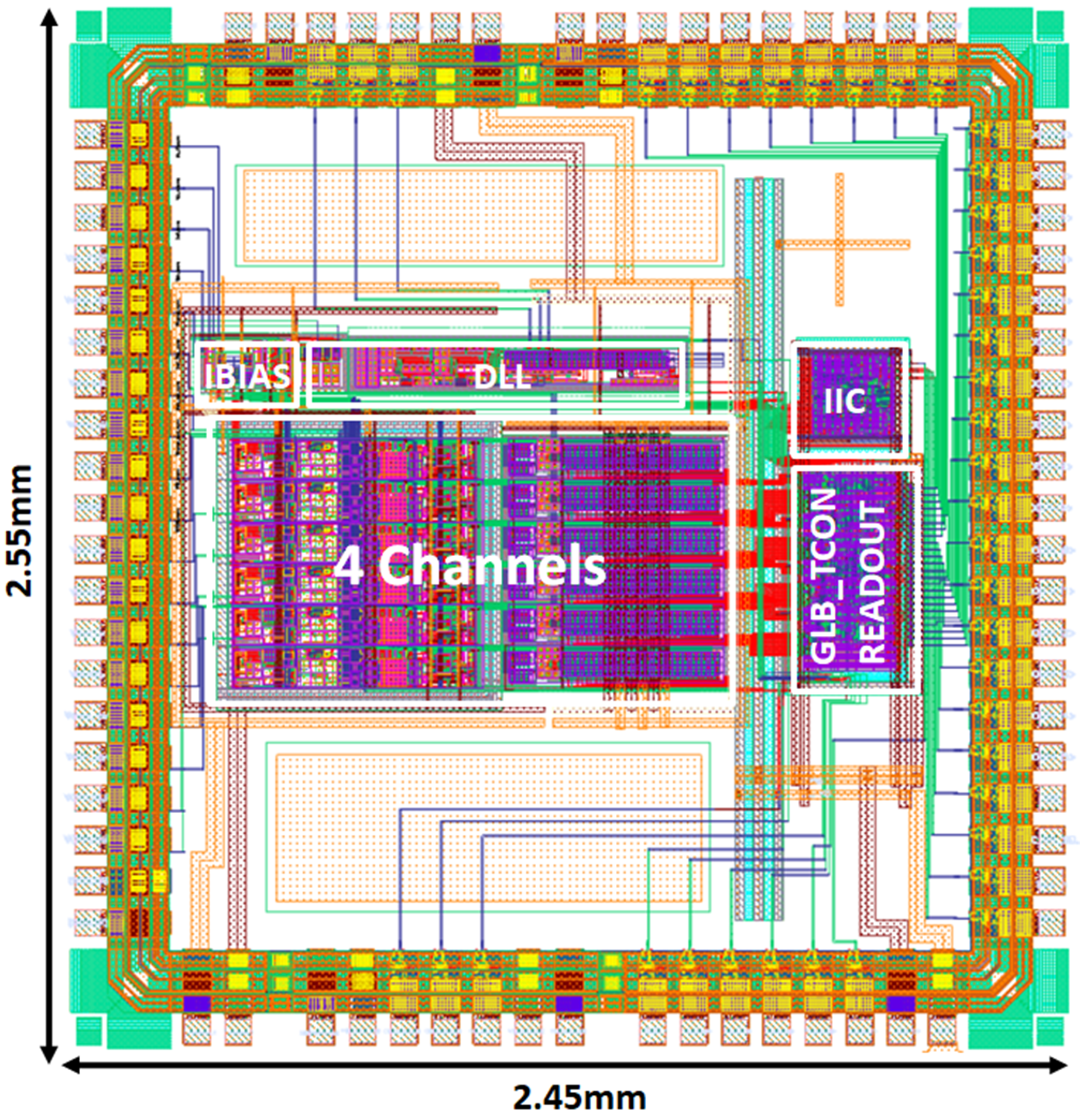
Fig.2 Layout of the fabricated chip
The layout is shown in Fig.2. The die size is 2.45 mm x 2.50 mm. The simulated results are obtained. The input dynamic range is 0.5 ~ 2.5V. The power is 4mW/channel. The sampling rate is 3.4 Msps without error codes. In the single-channel performance evaluation, the DNL is -1LSB/+0.7LSB and the INL is -3LSB/+2.5LSB. The ENOB is 12.7 bit. The above performance is benefit from the scheme of three-stage hybrid architecture. If the sampling rate is scarified, the resolution can be enhanced to 16 bit or larger. In addition, such architecture can be easily extended to multichannel applications, for example, 128 or 256 channels. This feature makes the proposed ADC a great potential in high-energy physics experiments and biomedical imaging applications.
The ADC has been taped out. The samples will come back soon. For future work, the ADC will be tested for the performance evaluation and a 16-channel ADC chip will be fabricated in the end of 2022.
(Authors: C. Yu, Reviewer: W. Gao)