Jitter Models of DLLs for Multiphase Clock Generation
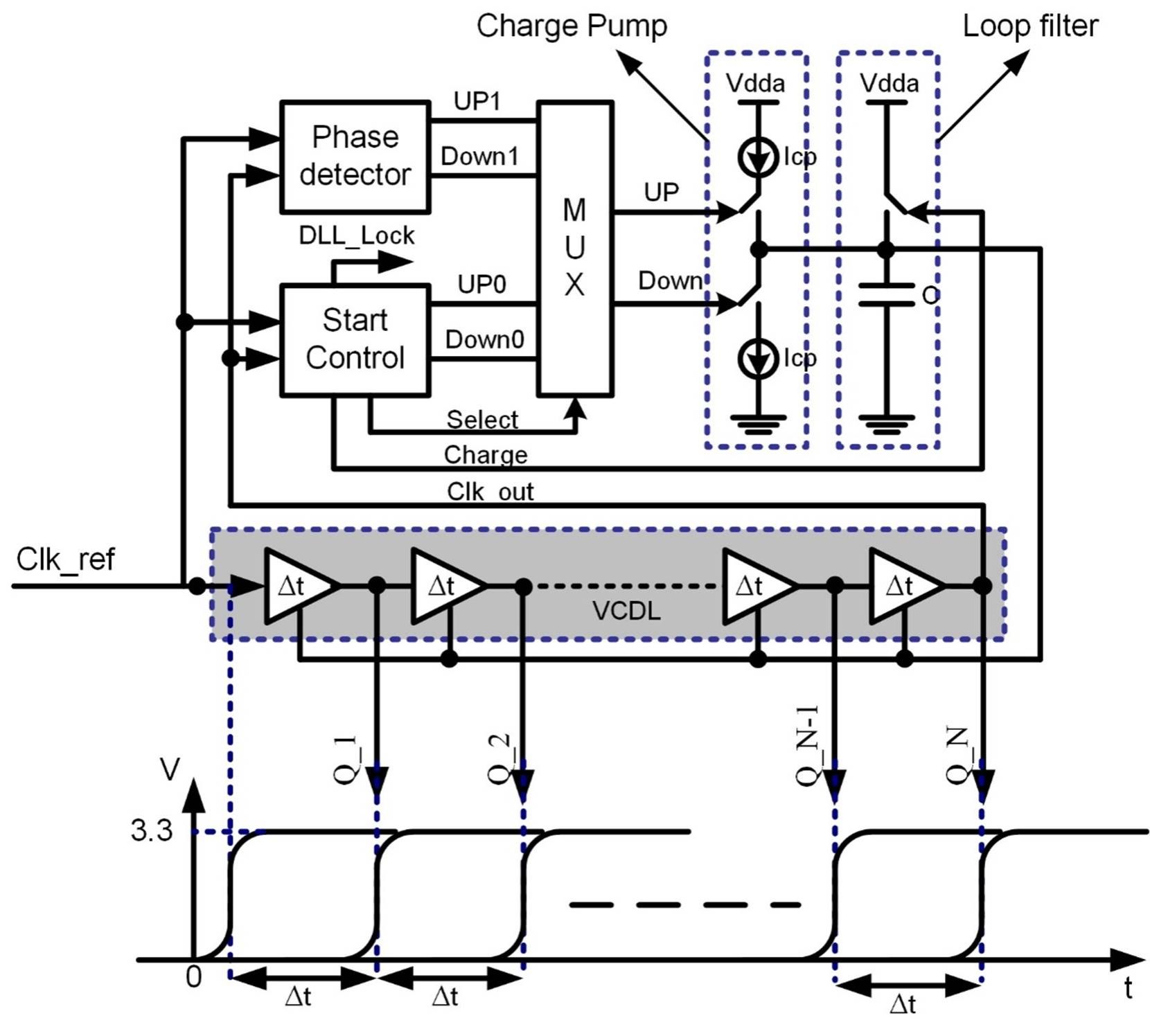
The schematic of a DLL is shown in Fig. 1. As usual, the DLL consists of a phase detector, a charge pump, a loop filter and VCDL. When the delay-locked loop (DLL) is employed as a timing generator, Clk_out and Clk_ref have a fixed latency of one clock period and the outputs of delay cells in voltage-controlled delay line (VCDL) are multiphase delayed clocks (Q_1, Q_2, …, Q_N).

Fig. 1 The schematic of a mixed-mode DLL
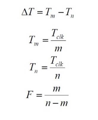
The architecture of an array of DLLs (ADLL) is shown in Fig.2. It can produce more phases in one clock period. Two kinds of DLL should be used to construct the array. The time taps of delay cells in both classes of DLL are Tm and Tn, respectively. The bin size of ADLL can be obtained by delay difference of Tm and Tn (where Tm > Tn). The ADLL should meet following condition.

where,
∆T is the bin size of ADLL.
Tclk is period of reference clock.
m and n are the numbers of delay cells in two kinds of DLL respectively.
F is the number of DLL with n delay cells.

Fig. 2 The architecture of an array of DLLs
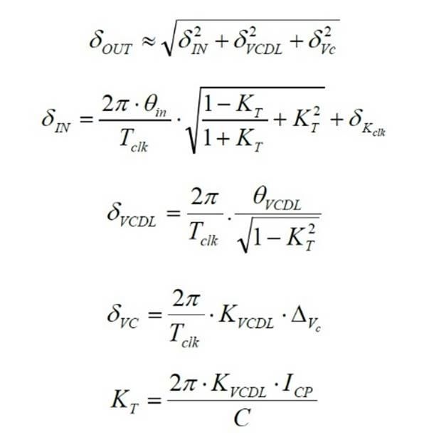
The jitter performance of the DLL should be taken into account to construct the above blocks. A jitter model has been given before the circuit design. In a mixed-signal charge-pump DLL, the jitter of the output clocks comes from input signal noise, circuit noise, and leakage current. The jitter of the output clock, the input clock, VCDL and controlled voltage (δOUT, δIN, δVCDL and δVC) are described as follows.

where,
θin is the input phase error caused by the signal noise and δKclk is the time error caused by the noise and the slope variation of the clock.
θVCD is the VCDL output phase error.
∆Vc is voltage noise of the capacitor(C) in loop filter.
KVCDL represents the gain of VCDL in s/V.
ICP is the charge and discharge current in the charge pump.
The VCDL and loop filter exhibit significant contributions to total jitter performances. Generally, the worst case jitter actually occurs at the last delay cell of the VCDL. The optimization of the jitter performance depends on the value of KT in the above models. To reduce the δOUT, KVCDL and ICP will be reduced or the value of capacitor (C) will be increased. By using this theoretical model, the RMS jitter of ~10 ps will be obtained by setting the value of KVCDL, ICP and C as 500 ps/V (when DLL is locked), 20 µA and 90 pF, respectively.