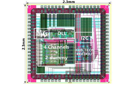
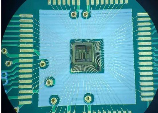
Since 2020, our group started a new project on the design of a multichannel event-driven single-slope ramp ADC for dark matter particle detection. The first prototype ASIC is designed in CMOS 180nm mixed-signal process. The chip has been back and now is under tested.
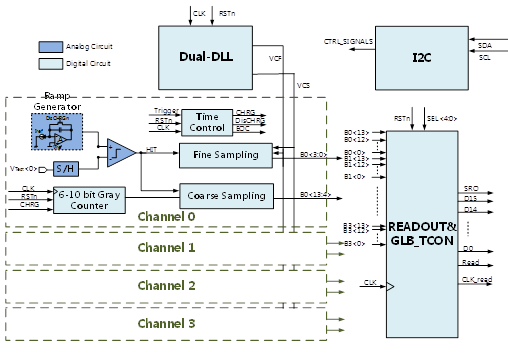
Four channel A/D conversion circuits are integrated in this ASIC. The blocks in each channel mainly include a ramp generator, a sample-and-hold circuit, a comparator, a counter, coarse and fine sampling circuits, and timing control circuits. All channels share a common readout control unit, a delay-locked loop (DLL), I2C interface and bias circuits. In order to quickly convert the peak voltage signals of front-end readout circuits and reduce the power consumption, a fully-customized event-drive mode is adopted to support the A/D conversion. In each channel, only one conversion is performed when an event arrives. In addition, the readout resolution of the ADC is programmable in order to meet the requirements of front-end readout circuits with different sampling rates. In this ADC, the resolution of 10 ~ 14 bits can be achieved though the configuration of the resolution of the counter and the integration time of the ramp voltage.
The ASIC prototype has been designed in 0.18μm CMOS mixed-signal 3.3/1.8 V process. The die size is 2.3 mm × 2.3 mm. The post-simulation results are listed in the following. The input voltage range is 0.5 ~ 2.5 V. The DNL is – 1 LSB ~ + 0.8 LSB. The INL is−3 LSB ~ + 1.5 LSB. The sampling rate is 100 kS/s ~ 3 MS/s. The power dissipation is 8 mW + 2.5 mW/channel. The ASIC is now under fabrication. The performance evaluation of prototype chips will be performed in this July.
A 16-channel ADC will be integrated with front-end readout circuits in a single ASIC in the next step.
(Authors: J.H. Geng, Reviewer: W. Gao)